Jfet Characteristics Circuit Diagram Jfet Oscillator Coupled
Electronic – how to determine drain and source resistor values for Draw the drain and transfer characteristics of jfet best drain photos Explain the structure and working of jfet. : electric guider
JFET-Junction Field Effect Transistor | Todays Circuits ~ Engineering
Jfet-junction field effect transistor Ohmic region on jfet characteristic curve P channel jfet circuit diagram
Jfet-junction field effect transistor,construction,symbol,operation
Jfet oscillator coupledJfet mosfet fet effect field junction vs diagram comparison transistor channel circuitstoday basic symbol transistors bjt gif schematic information credit Jfet circuit diagramIntroducción a los transistores de efecto de campo de unión (jfet).
Jfet transistor junction construction byjusJfet characteristics transfer explained Field-effect transistor (fet). junction field-effect transistor (jfetThe basic circuit of the source-coupled jfet oscillator..
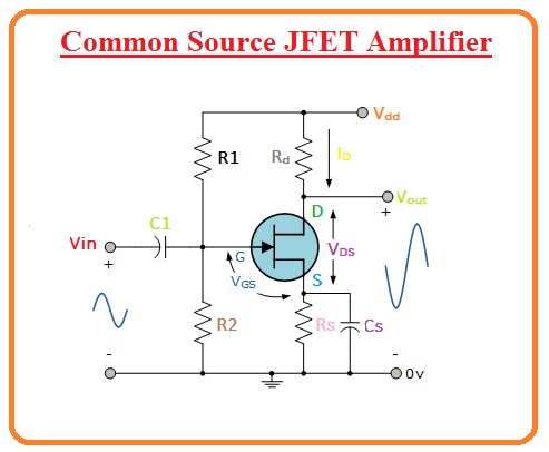
Jfet circuit diagram
Circuit diagram for jfet characteristicsJfet biasing method bias voltage divider biased Jfet, junction field effect transistor, jfet construction, jfet operationCharacteristics of jfet(drain and transfer characteristics) in english.
Junction field effect transistor or jfet tutorialSolved consider the jfet characteristics and the circuit Junction field-effect transistors (jfet) selection guide: typesJfet characteristic curve.

2n5457 n-channel jfet pinout, examples, features and datasheet
Jfet circuit diagramJfet circuit diagram Junction field-effect transistors (jfet): operation, characteristics2n5457 n-channel jfet : datasheet, working & its applications.
Jfet channel transistor schematic symbols effect field junction symbol diagram gate electronics operation source common drain configuration direction 2009 currentJfet schematic channel symbols field effect junction symbol transistor electronics circuit basics electrical drain choose board source construction Jfet circuit applications figure operation source channel configuration input commonTransistor curves fet characteristic junction output jfet field effect voltage gate source typical characteristics used jfets negative electronics ic mosfets.

[diagram] circuit diagram of jfet
12) jfet circuit diagram and its characteristicsJfet switch pinout datasheet example Jfet explainJfet circuit diagram.
Jfet circuit diagramJfet characteristic ohmic fet resistance variable Jfet n-channel and p-channel schematic symbolsJfet transistor polarity conventions effect field junction circuit operation construction symbol electronics.

Jfet transistor diagram
Jfet transfer characteristics explainedJfet characteristics channel transistor effect field junction ppt curve voltage characteristic fet online region Jfet biasing methodJfet: junction field effect transistor construction and working.
Jfet characteristics drain transfer .


